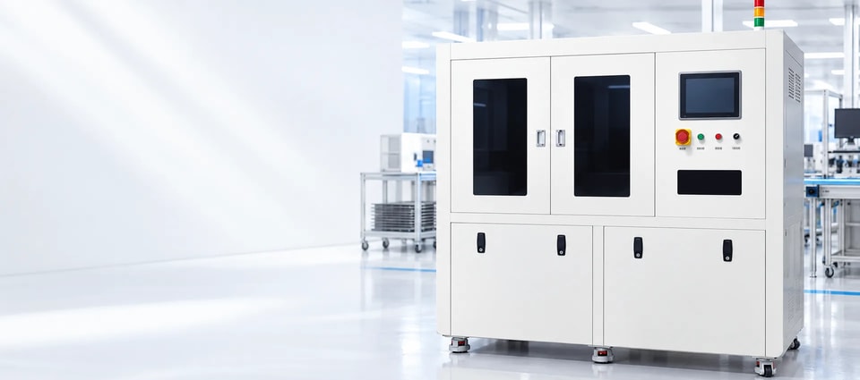
Plasma cleaning systems for semiconductor packaging
Clean you canmeasure.
RF and microwave plasma systems that remove micro-contamination and activate surfaces before wire bonding and encapsulation — engineered and built in Wuxi.
Selected customers
All customers




























Where plasma fits
Before the bond.
Before the seal.
Plasma cleaning removes micro-contamination and activates the surface at the steps where adhesion decides the result. Pick an application.
Clean pads and lead fingers for the wire — then activate the surface for the mold.
In IC packaging, plasma cleaning sits after die attach and cure, ahead of wire bonding, and again after bonding, ahead of molding.
- Die attach
- Cure
- 1Plasma
- Wire bond
- 2Plasma
- Molding
- Trim & form
- 1Before wire bond — removes surface contamination, for stronger ball-shear and stitch-pull
- 2Before molding — activates the surface for mold-compound adhesion, less delamination
A clean chip and frame before the wire goes on.
In LED packaging, plasma cleaning prepares the chip and lead frame before wire bonding, so the wire bonds reliably and the package holds together.
- Die attach
- Cure
- 1Plasma
- Wire bond
- Encapsulation
- 1Before wire bond — removes surface contamination and raises wettability
After sintering and before the gel — for DBC and AMB power modules.
In IGBT module packaging, plasma cleaning follows sintering, ahead of X-ray inspection and wire bonding, and follows bonding, ahead of potting.
- Die attach
- Sintering
- 1Plasma
- X-ray
- Wire bond
- 2Plasma
- Potting
- Test
- 1Before wire bond — clean chip and copper surfaces for heavy-wire bonding
- 2Before potting — stronger adhesion of the silicone gel
- Optical partsbefore coating
- PCBsbefore copper plating and assembly
- Glass and rubberbefore printing
- Engineering plasticsbefore coating
- Wafersphotoresist descum
- FlipChip packagesadvanced packaging
- Package shellsbefore wire bonding and sealing
- Biomedical devicessurface treatment
The line-up
Pick your format.
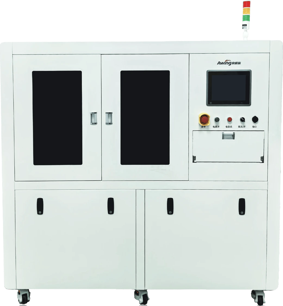
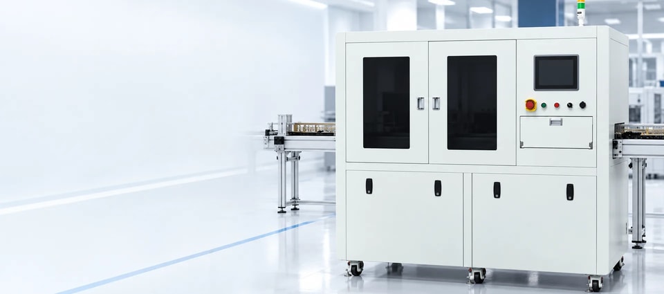
In-line RF plasma cleaner
AW-ZP
ZP04B · ZP04A
- Built around lead-frame strips
- Same-side or left-in / right-out loading
- Optional MES link
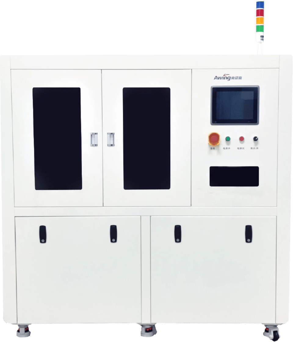
In-line microwave plasma cleaner
AW-ZMP
ZMP04
- No internal electrode in the chamber
- Uniform, gentle cleaning without ESD issues
- Shielded chamber
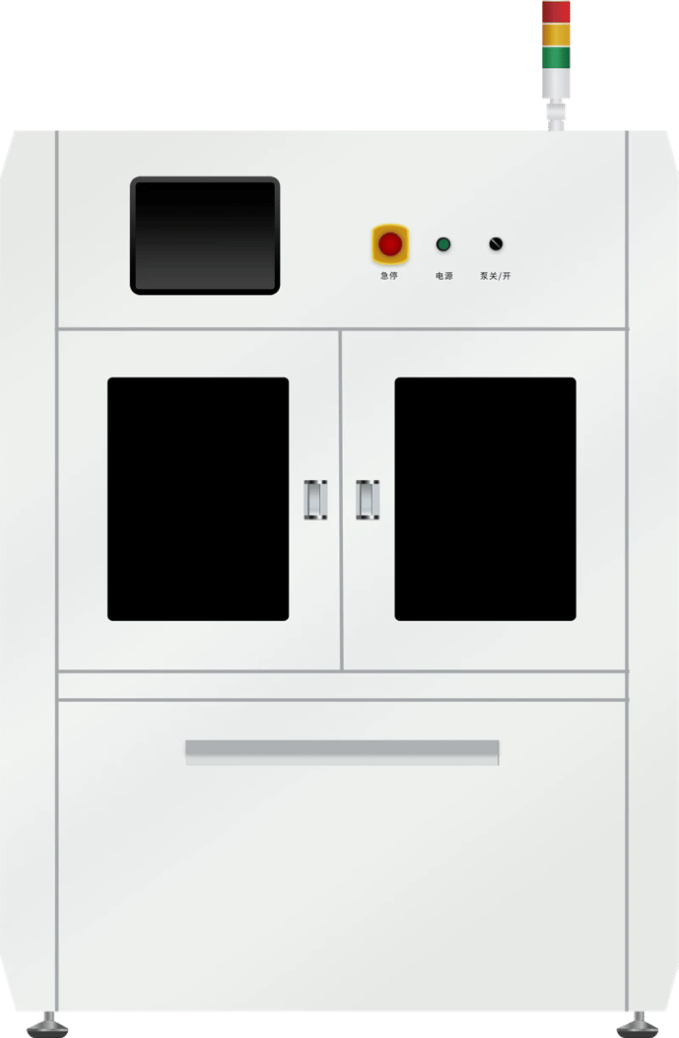
Continuous RF plasma cleaner
AW-LP
LP01
- Left-in / right-out line connection
- Tray-based transfer
- MES transmission
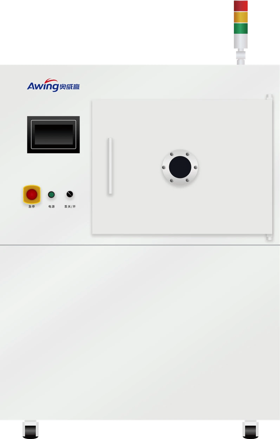
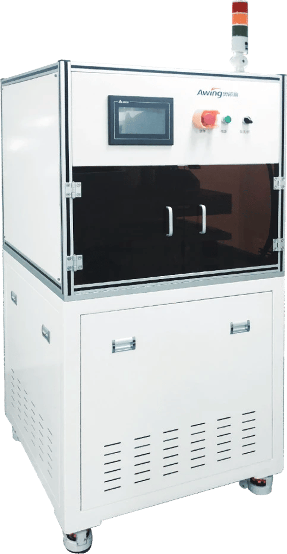
Chamber RF plasma cleaner
AW-P
P100 · P170
- Parallel or grid electrodes, adjustable spacing
- Stored recipes, full process control
- Optional automatic door
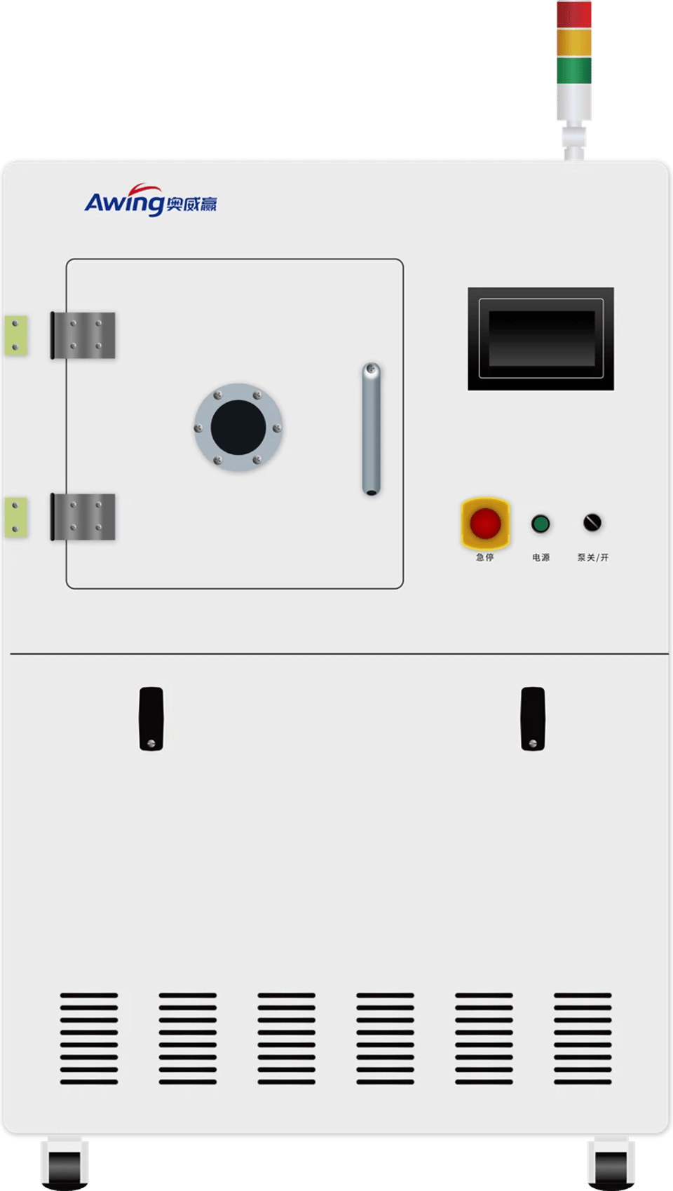
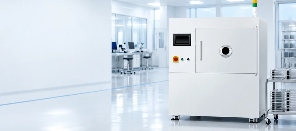
Chamber microwave plasma cleaner
AW-MP
MP60
- Rotating tray with ceramic microwave diffuser
- Friendly to ESD-sensitive parts
- Optional automatic door
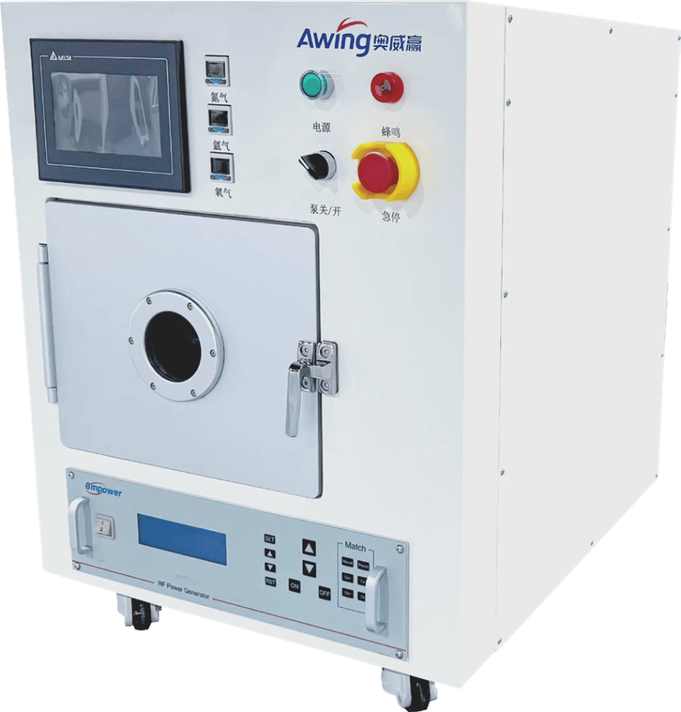
R&D chamber and benchtop RF cleaners
AW-P00X
P006 · P15
- Compact footprint for labs and R&D lines
- Modular benchtop with 1–5 electrode layers
- Stores 50 process recipes
In-line RF plasma cleaner
AW-ZP
ZP04B · ZP04A
- Built around lead-frame strips
- Same-side or left-in / right-out loading
- Optional MES link
Engineered and built in Wuxi.
About Awing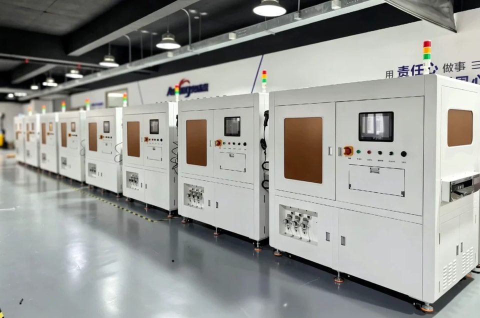
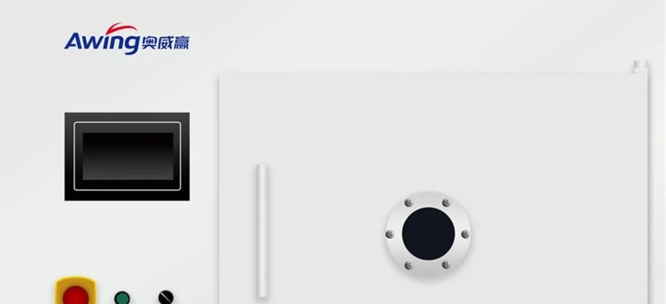
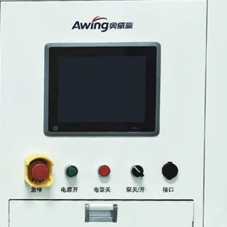
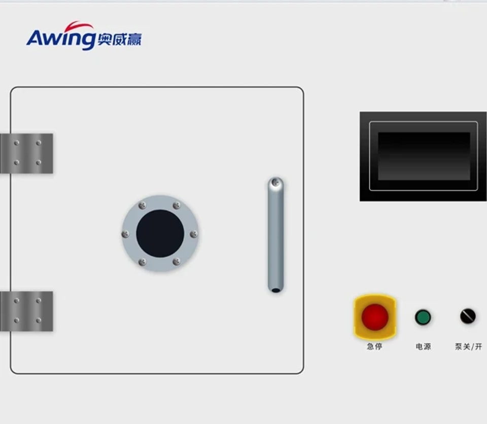
Since 2017, Wuxi Awing Technology has designed and built plasma cleaning systems for semiconductor packaging. A core team with 20+ years in plasma process research, 40+ granted patents and more than 200 customers across IC packaging, power devices, optical communication and automotive electronics.
- ISO 9001quality managementto 2029-04
- ISO 14001environmental managementto 2028-06
- ISO 45001occupational health & safetyto 2028-06
- CEcertificate of conformityto 2027-01
- National High-tech EnterpriseChinato 2027-11
- Specialized & Innovative SMEJiangsu Provinceto 2028-12
- After-sales servicecertificationto 2029-06
What buyers ask first.
Short answers to the questions process engineers and buyers bring to the first call.
All buyer questionsQ1RF or microwave plasma — which suits my parts?
Both remove surface contamination and activate the surface before bonding or molding. Awing's microwave systems (2.45 GHz) have no internal electrode in the chamber, so nothing but the process gas is present there — gentle on ESD-sensitive parts. RF systems (13.56 MHz, automatic impedance matching) cover the widest range of formats, from in-line strip cleaners to benchtop units. Tell us your substrate and we will recommend the source.
Q2In-line or batch chamber — when does each make sense?
In-line systems (AW-ZP, AW-ZMP) take lead-frame strips automatically, with same-side or left-in / right-out loading and an optional MES link — built for packaging lines. Batch chambers (AW-P, AW-MP) treat trays and fixtures on multi-layer electrodes or a rotating tray, with stored recipes and electrode spacing that adjusts to the workpiece — suited to mixed parts and larger pieces. The continuous AW-LP links up- and downstream equipment.
Q3How do you prove a surface is clean?
With measurements, each against a specification: water contact angle (qualification spec below 30°), wire-bond ball-shear and stitch-pull strength against their lower spec limits, and Cu residue after ball shear (above 75%). Example qualification data is on our test methods page.
Q4What do you need from us for a quotation?
Your package or substrate type, strip or part dimensions, the contamination or process step to treat, target throughput (UPH) and how the system joins your line — standalone, left-in / right-out, or with an MES link. Drawings or photos help us propose the right format.
Latest from Awing.
All newsWarm congratulations to Wuxi Awing Technology Co., Ltd. on being recognized as a Wuxi Municipal Enterprise Technology Center
ReadWuxi Awing Technology invites you to a major semiconductor industry event in Wuxi on September 4
ReadWarm congratulations to our company on passing the 2025 Jiangsu Province Specialized and Innovative SME recognition
ReadStart with your process
Tell us the part.
We'll suggest the system.
04Your contact

Inquiry
Send us a message.
Fields marked * are required. Details about the part, the material and the process help an engineer give a useful first reply.