
Application · Semiconductor packaging
Clean pads. Stronger bonds.
In IC packaging, plasma cleaning sits at two points in the line: after die attach, ahead of wire bonding — and after bonding, ahead of molding. It removes surface contamination and activates the surface for the wire and the mold compound.
Where plasma fits
Before the bond.
Before the seal.
In IC and power-module packaging, plasma cleaning sits at two points in the line: after die attach, ahead of wire bonding — and after bonding, ahead of molding or potting.
IC packaging
- Die attach
- Cure
Plasma
- Wire bond
Plasma
- Molding
- Post-mold cure
- Trim & form
IGBT power modules
- Die attach
- Sintering
Plasma
- X-ray
- Wire bond
Plasma
- Potting
- Forming
- Test
- Marking
01 · before the bond
Clean pads and lead fingers for the wire.
- Removes surface contamination
- Raises surface energy and wettability
- Higher ball-shear and stitch-pull strength
- Fewer weak or non-stick bonds
02 · before the seal
An active surface for mold compound and gel.
- Stronger adhesion of mold compound and potting
- Less delamination
Plasma is also used to clean carriers before die attach, before coating optical parts and engineering plastics, before printing on glass and rubber, for photoresist descum, and to treat biomedical devices.
Four formats, one process.
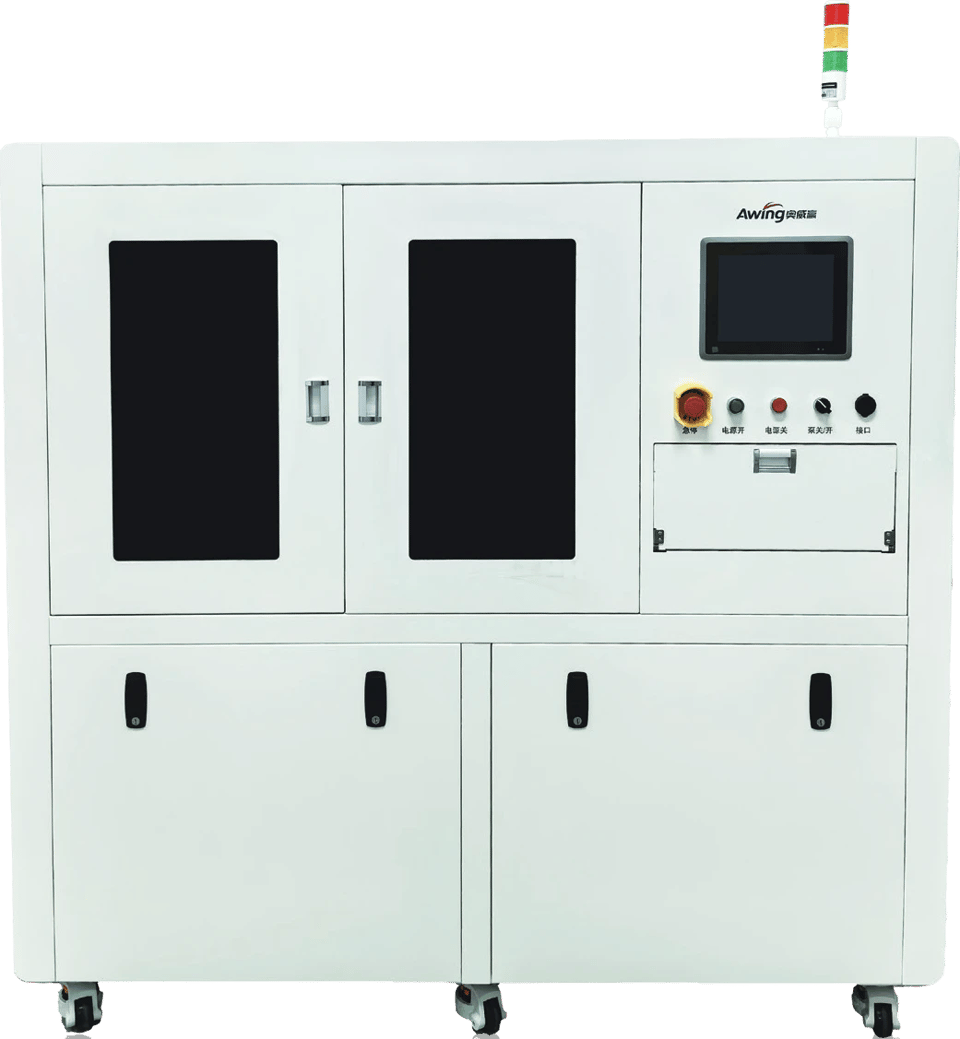
AW-ZP04B · in-line RF
Lead-frame strips L 150–300 × W 30–100 mm, 4 lanes × 4 strips, UPH above 500.
AW-ZP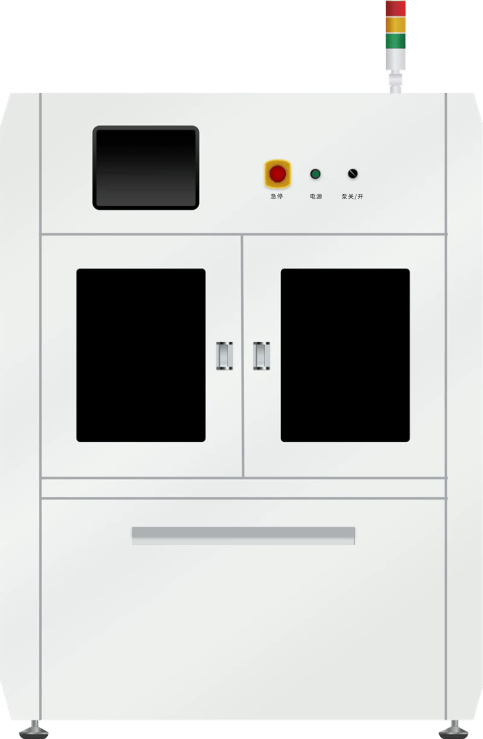
AW-LP01 · continuous RF
Tray transfer with left-in / right-out connection to the tools around it.
AW-LP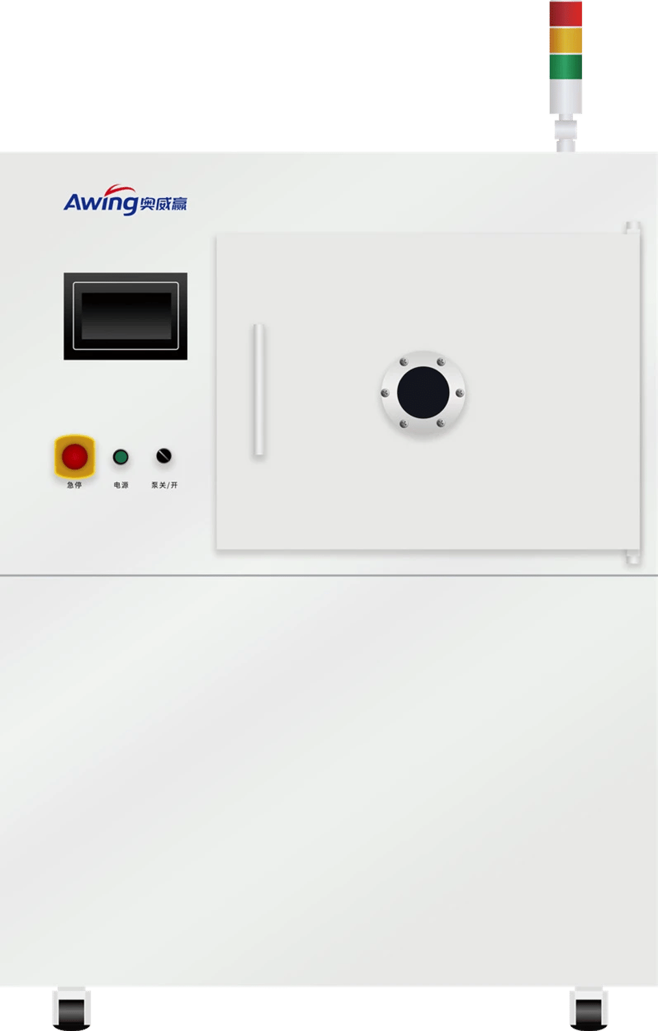
AW-P · chamber RF
Batches of trays and fixtures on multi-layer electrodes, P100 and P170.
AW-P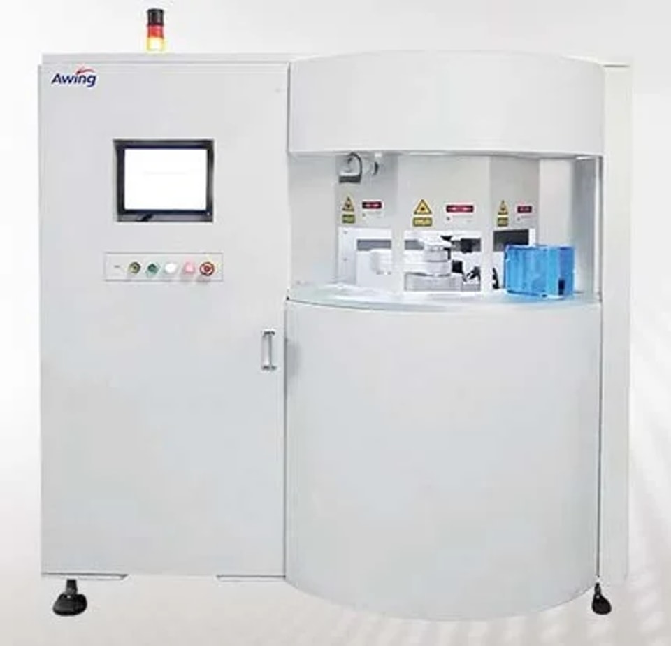
AW-QP600 · wafer descum
Photoresist strip and descum for 4-, 6- and 8-inch wafers.
AW-QPVerification
Measured, not assumed.
A clean surface is proven with measurements, each against a specification: water contact angle below 30°, ball shear above 40 g, stitch pull above 10 g and Cu residue after ball shear above 75%.
In Awing's qualification data, the water contact angle fell from 81.2° to 16.1° after plasma cleaning.
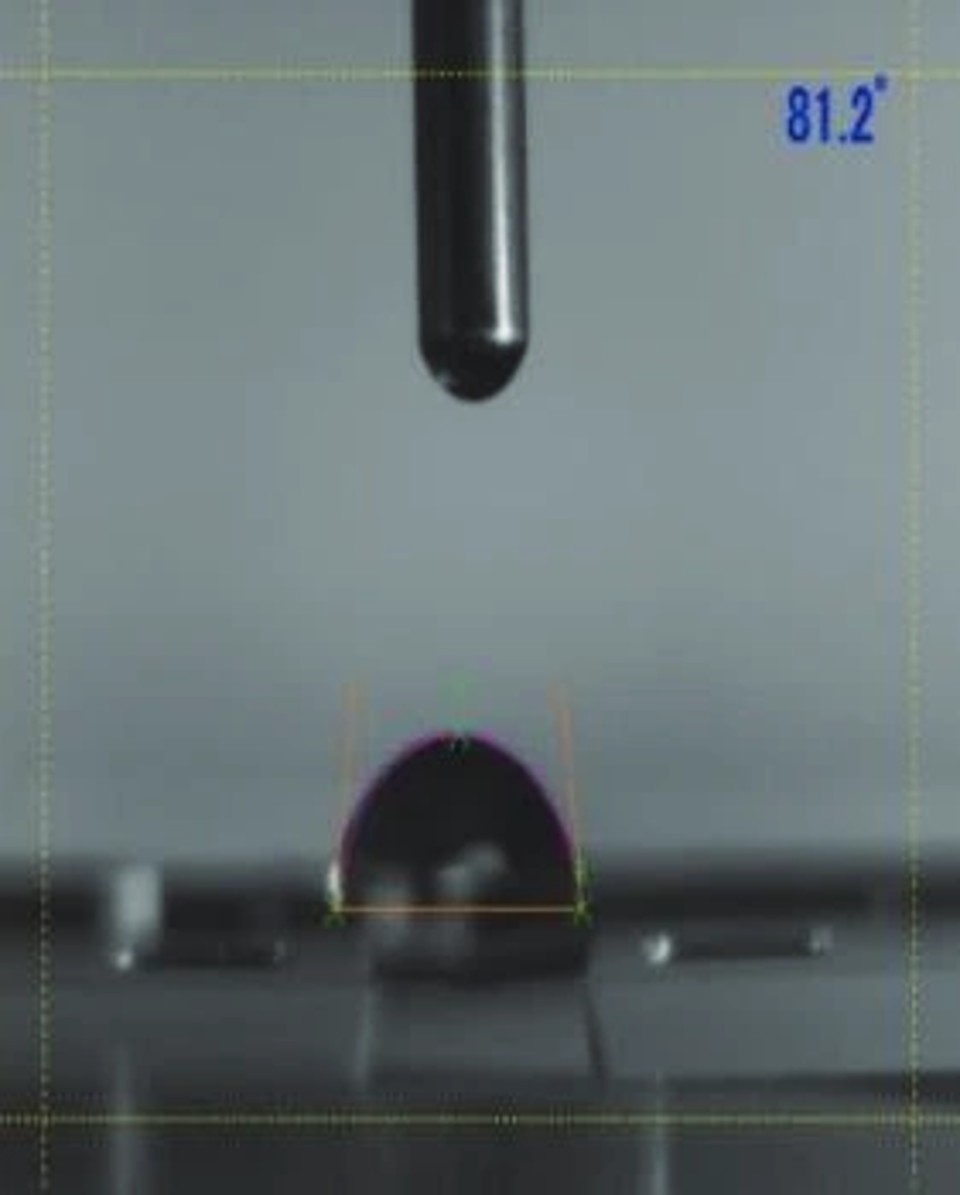
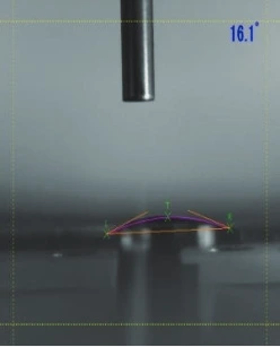
Water contact angle before and after plasma · Awing qualification data
Semiconductor packaging, briefly.
Q01What does plasma cleaning remove before packaging?
Surface contamination on pads, lead fingers and substrates that would weaken wire bonds or the adhesion of mold compound. Plasma removes it and activates the surface; the gas and recipe are chosen for the contamination and the substrate.
Q02Where in the line does it go?
After die attach and cure, ahead of wire bonding — and after wire bonding, ahead of molding. In IGBT modules the same two positions sit before wire bonding and before potting.
Q03In-line or chamber for my line?
In-line systems take lead-frame strips straight from the line; chambers treat trays and fixtures in batches. Compare the formats.
Tell us the strip.
Strip dimensions, target UPH and how the system joins your line. A process engineer recommends the series and lists what else we need to quote.

Inquiry
Send us a message.
Fields marked * are required. Details about the part, the material and the process help an engineer give a useful first reply.